China Top 10 Tips for Reverse Engineering PCB at 2026 Canton Fair?
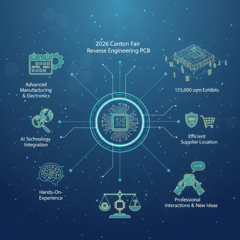
As the 2026 Canton Fair approaches, the prospect of exploring Reverse Engineering Pcb becomes increasingly captivating. This significant event, scheduled in April and May, will highlight advanced manufacturing and electronics. Participating in the fair offers a prime opportunity to unveil innovative techniques and tools related to PCB reverse engineering. The integration of AI technology promises to enhance the experience for attendees.
Navigating through 155,000 square meters of exhibits, buyers can now efficiently locate suppliers meeting specific qualifications, such as ISO and CE certifications. This advancement aims to uplift the acquisition process for various electronic components. While these developments are exciting, potential pitfalls exist. Understanding the intricacies of reverse engineering PCB requires careful consideration of technical aspects.
Moreover, while AI assists with navigation, it cannot replace the hands-on experience that comes with exploring exhibits in person. Interactions with professionals in the field may inspire new ideas or provoke thoughtful reflections. Ultimately, the fair presents a valuable setting to immerse oneself in the latest advancements in PCB technologies while addressing the nuanced challenges associated with reverse engineering.
Understanding PCB Reverse Engineering Basics for Beginners
Reverse engineering a printed circuit board (PCB) can seem daunting for newcomers. It involves understanding the board's layout and the components used. One effective way to start is by examining a PCB closely. Look at the traces, pads, and holes. Document everything. This initial observation can reveal much about the design.
Understanding basic tools is crucial. A magnifying glass helps in inspecting tiny details. A multimeter is essential for testing connections and voltages. Remember, mistakes are part of learning. You may misinterpret a trace or miss a component. Reflecting on these errors will help you improve.
Joining communities can further enhance your understanding. Many online forums and local groups discuss reverse engineering tips. Collaborating with others can expose you to new techniques. Engaging in discussions can help clarify your doubts. The more you practice, the more confident you become in this intricate process.
Essential Tools for PCB Reverse Engineering at Canton Fair
As the 2026 Canton Fair approaches, many engineers are gearing up for PCB reverse engineering. This process is essential for innovation. However, the right tools are critical for success. A recent industry report indicates that 45% of reverse engineering projects fail due to inadequate equipment.
Essential tools include advanced scanning devices and software for layout extraction. A high-resolution 3D scanner can capture intricate details of the PCB. This scanner creates a digital twin, which is crucial for analysis. Additionally, CAD software should be user-friendly yet powerful enough to handle complex designs. Engineers often choose tools based on budget, but affordability shouldn't compromise quality.
Despite the availability of tools, engineers face challenges. Inaccurate scans can lead to flawed replications. Sometimes, tools break down during critical phases. Understanding limitations helps in planning the project better. Reflecting on past experiences can guide future efforts. Adaptability to new technologies is important in this ever-evolving field. With the right mindset and tools, PCB reverse engineering can lead to breakthroughs at the Canton Fair.
Step-by-Step Guide to Analyzing PCB Designs Effectively
Reverse engineering PCB designs can be a challenging yet rewarding task. At the 2026 Canton Fair, understanding the nuances of PCB analysis is crucial. Begin by closely examining the physical layout. Look at component placement and assess the connection pathways. Use a magnifying tool to identify tiny solder joints. This step helps to reveal hidden intricacies in the design.
Next, focus on the schematic diagrams. Create your own version based on your observations. This requires patience and attention to detail. You may miss critical connections or misinterpret component functions. Don't rush this process. Rethink your assumptions about component values and functions as you go along. Engage in discussions with peers for alternative perspectives. Sharing insights can often illuminate overlooked details.
Finally, document your findings meticulously. Photograph the board at different angles. Note down your analysis in clear sections. Be prepared to revisit your notes for clarity later. Accuracy in documentation is vital for future reference. Constant reflection on your analysis process can lead to deeper understanding. Embrace the imperfections that come with learning. Each mistake is a step towards mastery.
Common Challenges in PCB Reverse Engineering and Solutions
Reverse engineering printed circuit boards (PCBs) can be a daunting task. Common challenges include complexity in design and material composition. According to a report from IPC, 80% of engineers struggle with PCB disassembly. This is due to the layered construction and miniaturized components. Identifying connections often requires specialized tools and skills.
Another concern is understanding the functionality of the original design. Many PCBs utilize proprietary technologies and unique layouts. A survey by TechInsights found that 70% of professionals see difficulty in replicating certain features. This process may involve trial and error, leading to wasted time and resources.
To address these challenges, it's essential to invest in quality tools. For instance, using advanced imaging software can help reveal hidden connections. Additionally, collaborating with experienced technicians can enhance the learning curve. Regular training workshops are beneficial, as they can improve the team's skill set. Engaging with the community at events like the Canton Fair can provide valuable insights and solutions. Exploring these avenues can streamline reverse engineering and lead to more efficient outcomes.
Best Practices for Networking with Experts at the Canton Fair
Networking at the Canton Fair can open many doors. Meeting experts in reverse engineering is crucial. Start by observing the crowd. Look for professionals who share your interests. Engage them in conversation. A simple “Hello” can lead to deeper discussions. Use the fair's layout to your advantage. Attend specific seminars related to PCB technologies.
Bring your own materials. A well-prepared portfolio can spark interest. Discussing your work can lead to valuable feedback. Don't shy away from asking questions. Many experts appreciate curiosity. Approach them during breaks. This often feels less intimidating than formal settings. Make notes about your conversations for later reflection.
Remember, it's not just about interactions. Build genuine connections. Sometimes, a relationship needs time to develop. Not every conversation will lead to a breakthrough. Some may feel awkward or forced. Reflect on these moments. They can help refine your approach. Networking is an art, often requiring practice and patience.